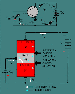
 It struck me today that a modern investment bank can be modelled as a transistor. Specifically, an investment bank in a state of liquidity corresponds to a transistor which is switched on, and an investment bank in a state of bankruptcy corresponds to a transistor which is switched off.
A pnp transistor consists of two p-type semiconductors sandwiching a narrow n-type semiconductor. One p-type region is the 'emitter', the other is the 'collector', and the filling in the sandwich is the 'base'. A terminal is attached to each. A voltage Vcc is applied across a circuit which contains the emitter-base-collector as a component, and this voltage places the emitter at a higher potential than the collector. A smaller second voltage is placed across the emitter-base only. The voltage across the emitter-base is the input voltage Vin, and the combined result of Vcc and Vin is a voltage across the emitter-base-collector, which is the output voltage Vout. There will no current across the emitter-base-collector until the input voltage is increased to a critical value, at which point the current is switched on, with a corresponding voltage Vout across the emitter-base-collector much larger than Vin. Hence, by this means, a transistor acts as both an amplifier and a switch.
A modern investment bank made long-term investments using some of its own capital, but mainly by using loans taken from other financial institutions, whom we can refer to as the primary lenders. These loans were typically paid off with a combination of returns from the long-term investments, and loans from other financial institutions, whom we can refer to as secondary lenders.
Now, I propose that the investment bank corresponds to the base in a transistor, the investment assets correspond to the emitter, and the primary lenders correspond to the collector. The flow of money back to the bank from the long-term investments, and on to the primary lenders, corresponds to the flow of current between the emitter and the collector in a transistor. The flow of money back from the long-term investments, and on to the secondary lenders, corresponds to the flow of current produced by the input voltage across the emitter-base in a transistor. As long as the voltage across the emitter-base is above the critical threshold value, a current will flow from the emitter, through the base, and on to the collector. Similarly, as long as the secondary lenders have sufficient confidence in the flow of money from the investment assets back to the bank, and on to themselves, they will lend money to the investment bank which enables the bank to pay off its primary loans. The voltage across the emitter-base corresponds to the level of confidence the secondary lenders have in getting a return on their loan. However, if their confidence drops below a critical threshold, they will cease lending the bank money, and there will be an insufficient flow of money from the long-term investments alone to pay off the primary lenders. At this point the investment bank becomes bankrupt. In effect, the transistor switches off.
One of the remedies proposed in the wake of this year's global financial collapse, is to improve the mathematical models of systemic risk within the financial industry. If this transistor analogy has sufficient validity, then perhaps one could model an entire financial system as an integrated electronic circuit board, and one could model systemic risk in this manner.
Just a thought...
No comments:
Post a Comment
Note: only a member of this blog may post a comment.